
THEBUSINESSBYTES
BUREAU
BHUBANESWAR,
APRIL 18, 2026
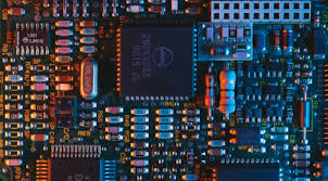
In a landmark boost
to India’s semiconductor ambitions, Odisha is set to host the country’s first
advanced 3D glass semiconductor packaging unit, with the groundbreaking
ceremony of the Heterogenous Integration Packaging Solutions (3D Glass
Solutions) scheduled in the capital city on Sunday.
The ambitious
project, backed by an investment of ₹1,943 crore, is poised to position Odisha as a global
hub for next-generation semiconductor manufacturing. The state government
described the initiative as a transformative step that brings the world’s most
advanced chip packaging technology to India for the first time.
 The foundation-laying
ceremony will be attended by Chief Minister Mohan Charan Majhi, Union Minister
for Electronics & IT Ashwini Vaishnaw, and Odisha’s Electronics & IT
Minister Mukesh Mahaling, along with senior government officials, global industry
leaders, investors, and members of academia.
The foundation-laying
ceremony will be attended by Chief Minister Mohan Charan Majhi, Union Minister
for Electronics & IT Ashwini Vaishnaw, and Odisha’s Electronics & IT
Minister Mukesh Mahaling, along with senior government officials, global industry
leaders, investors, and members of academia.
Once operational, the
facility is expected to generate around 2,500 direct and indirect employment
opportunities, while achieving an annual production capacity of 50 million
assembled semiconductor units. The chips developed at the unit will cater to
critical and high-growth sectors such as aerospace, defence, artificial
intelligence, 5G technologies, and data centres.
Industry experts believe the project will significantly strengthen India’s position in the global semiconductor value chain, particularly in advanced chip packaging — an area crucial for powering next-generation electronics.
With this development, Odisha becomes the first state in the country to host both a compound semiconductor fabrication unit and a cutting-edge 3D chip packaging facility based on glass substrates, marking a decisive stride towards building a robust semiconductor ecosystem in the country.