
THEBUSINESSBYTES BUREAU
BHUBANESWAR, MAY 29, 2026
In a landmark development that could redefine India’s eastern technology
landscape, the Odisha Government on Friday announced that Intel Corporation and
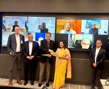
3D Glass Solutions (3DGS) have signed a Memorandum of Understanding (MoU) to
explore the establishment of a world-class advanced semiconductor glass core
packaging substrate manufacturing facility in the state.
The proposed project, subject to necessary approvals, funding support
from the State and Central Governments, and other business and regulatory
conditions, is being viewed as a transformative opportunity that could propel
Odisha into the league of emerging global semiconductor and advanced technology
hubs.
If realized, the facility would rank among the most significant
technology investments in Eastern India and would strategically position Odisha
as a major centre for semiconductor manufacturing, advanced packaging
technologies, artificial intelligence infrastructure, next-generation data
centres, and cutting-edge digital innovation.
The announcement marks a major milestone in Odisha’s ambitious push to
emerge as a key player in India’s fast-growing semiconductor and electronics
ecosystem, aligned with the national vision of technological self-reliance and
global competitiveness.
The Odisha Government also extended an open invitation to ecosystem
partners, technology leaders, research institutions, and industry stakeholders
across the world to participate in building what it described as one of Asia’s
most advanced semiconductor and digital infrastructure ecosystems.
Babu Mandava, CEO, 3D Glass Solutions, said, “We are grateful for the
strong support of the Government of Odisha and excited about our collaboration
with Intel in exploring this opportunity. This initiative has the potential to
establish India as a key global hub for advanced glass substrates and
semiconductor packaging, supporting high-growth sectors such as artificial
intelligence, high-performance computing, and next-generation electronics.”
Naga Chandrasekaran, Executive Vice President and General Manager, Intel
Foundry, said: “Intel Foundry is proud to collaborate with 3DGS in exploring
this opportunity with the Government of Odisha. As a pioneer in glass core
substrate technology, we are excited about the potential of this collaboration
to accelerate the commercialization of next-generation advanced packaging
solutions globally.”
Industry observers believe the proposed initiative could significantly
strengthen India’s semiconductor supply chain ecosystem while creating
substantial opportunities for high-value manufacturing, research and
development, innovation-driven entrepreneurship, and skilled employment
generation.
Odisha’s proactive industrial policies, integrated infrastructure,
expanding talent pool, and strategic focus on electronics and digital
industries are increasingly attracting global technology investments. The
proposed semiconductor packaging substrate facility is expected to further
reinforce the state’s reputation as a preferred destination for advanced
manufacturing and emerging technologies.
Odisha Chief Minister Mohan Charan Majhi described the initiative as a
defining moment in the state’s economic and technological transformation
journey.
The Chief
Minister said: “Today marks the beginning of a new chapter in Odisha’s growth
story. This initiative goes beyond semiconductor manufacturing — it is about
creating a future where Odisha becomes a globally competitive destination for
advanced technologies, innovation, AI infrastructure, data centres, and digital
transformation.
Our vision is to build a vibrant ecosystem that inspires future
generations, creates world-class opportunities for our youth, attracts leading
global technology companies, and firmly places Odisha on the global
semiconductor map. This is a transformational, generational opportunity that
will accelerate economic growth, strengthen India’s technological
self-reliance, and position Odisha at the forefront of the global digital
economy.”
The development also reflects the Centre’s broader push to strengthen
domestic electronics manufacturing and reduce dependence on imports by creating
a globally competitive semiconductor ecosystem within the country.
Dr. Mukesh Mahaling, Minister Electronics and Information Technology, Health
and Family Welfare and Parliamentary Affairs, Government of Odisha, said:
“Odisha remains focused on building a conducive ecosystem that promotes
innovation, facilitates investments, creates job opportunities, and drives
inclusive growth across industries.”
Ashwini Vaishnaw, Union Minister Electronics and Information Technology,
Railways and Information and Broadcasting, Government of India, stated: “This
initiative reflects India’s larger vision of strengthening domestic
manufacturing capabilities and positioning the country as a global economic
powerhouse.”
Odisha Chief Secretary Anu Garg said: “This MoU marks a transformative
step in Odisha’s journey towards becoming a key player in advanced
semiconductor and electronics manufacturing. With strong policy support,
skilled talent, and integrated infrastructure, Odisha is ready to contribute
meaningfully to India’s semiconductor ambitions.”
Aligned with Odisha Vision 2036 and India’s vision of Atmanirbhar Bharat, the initiative reinforces the state government’s commitment to building a globally competitive semiconductor, electronics, AI, and digital infrastructure ecosystem capable of serving both national priorities and global markets in the coming decades.
With semiconductor technologies becoming increasingly central to the future of artificial intelligence, cloud computing, automotive electronics, telecommunications, and high-performance computing, the proposed collaboration between Intel and 3DGS is expected to significantly elevate Odisha’s profile in the global technology and innovation landscape.